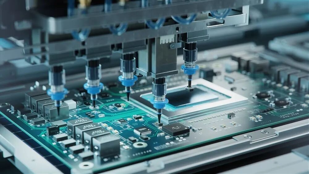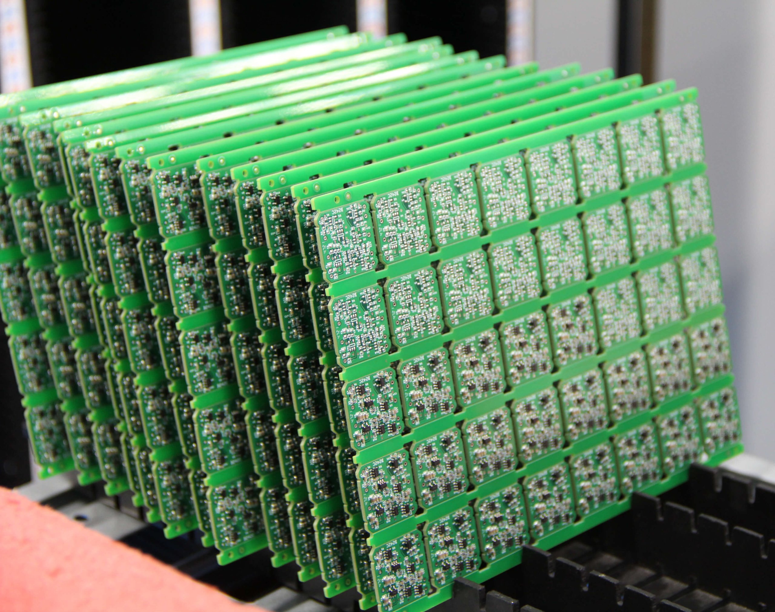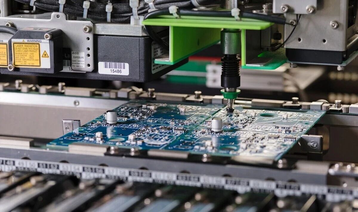

PCB panelization is to combine multiple smaller circuit boards of similar shape to form a larger PCB surface. The purpose of doing this is to reduce the loss of the board, that is, to improve the utilization rate of the PCB board; another reason is to increase the output efficiency of SMT patches.
Common types of puzzles
V-CUT panel: Cut a V-shaped groove between two PCBs, the gap is generally 0.4mm, and it is easy to break. The edges of the two boards need to be merged together when paneling. Suitable for regular PCB boards, convenient for mechanical or automatic panel separation.
Notes:
The thickness of the PCB for paneling should be ≤3.5mm.
For PCBs that require automatic panel separation by machine, both sides of the V-CUT line are required to retain a component no-layout area of not less than 1mm.
Considering the safety distance "S" from the edge of the V-CUT to the edge of the line (or PAD), S is generally required to be ≥0.3mm.
Stamp hole panel: The edges of the two boards are connected by a small piece of board, and there are many small holes at the connection, which is easy to break. After breaking, the edge of the board is like the edge of a stamp. Suitable for irregular PCB boards.
Notes:
The stamp hole should be a non-metallized hole with a hole diameter of 1mm and a center distance of 1.6~2mm between holes.
The stamp holes should be evenly distributed around each panel to avoid deformation of the PCB due to uneven force during welding.
What is the significance of a PCB Mirror-Board?
Mirror-Board refers to placing the front and back of the same PCB on the same panel, that is, mirroring the front and back designs of a PCB on a panel. This design method is often used for circuit boards with fewer parts, such as mobile phone PCBs, to fully utilize the capacity of the SMT production line and improve production efficiency.
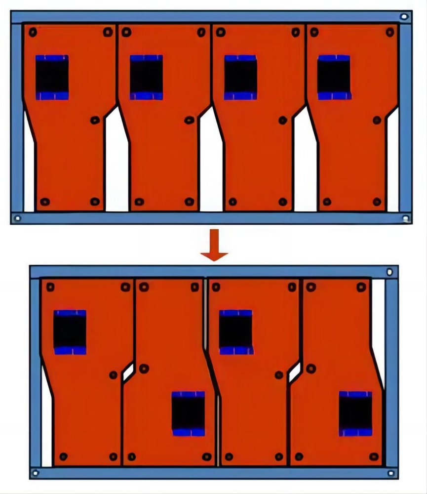
Mirror-Board design can improve production efficiency because it allows the components on both sides to be mounted simultaneously in one production process, saving time and cost, and making better use of board space and reducing waste. However, it also has some disadvantages, such as the complexity of mounting and the problem of uneven heat. The position and orientation of certain components may increase the difficulty of mounting, and the heat capacity of different components may cause uneven heat during the reflow process, requiring special thermal management measures.
What does PCB process edge mean?
The process edge of the PCB is to add 5mm width on both sides or four sides of the board. The main function is to reserve the track transmission position for the SMT placement machine so that the PCB board can be accurately clamped and transferred by the machine.
Components that are too close to the track edge are prone to collision when the SMT placement machine suction nozzle picks up the components and mounts them on the PCB board, and production cannot be completed. Therefore, a certain process edge must be reserved. Similarly, it is also applicable to some plug-in components to prevent similar phenomena when passing through wave soldering.
The process edge is not part of the PCB board and will be removed after production. With the panelization and process edge design, there is no need to make a jig. Not making a jig means saving pre-production preparation time, so that delivery can be faster.
Factors to consider when designing a panel
Panel size:
Different patch factories have different requirements for the maximum and minimum sizes of panels. Generally speaking, PCBs smaller than 50x50mm are recommended to be panelized to improve production efficiency. The maximum size that Pulin Circuit can panelize is: double-sided board ≤1400*610mm, multi-layer board ≤1050*610mm.
Consider the border and gap of PCB:
Reasonably set the gap and border between PCBs to facilitate cutting and assembly, while ensuring that they will not be damaged during separation due to too small gaps.
Component spacing and layout:
Ensure that the components on each small PCB are reasonably arranged to avoid interference between components, and at the same time ensure that the components between PCBs do not affect each other.
Component arrangement and splitting stress:
When designing the panel, the arrangement of components should avoid component cracking caused by splitting stress. The pre-marked panel structure can minimize the warping deformation during panel separation and reduce the stress on the components. Try not to arrange valuable components next to the process edge to avoid damage during panel separation.
Panel size and form:
The size and form of the panel should be processed according to the specific project requirements, and the appearance design should be as close to the square as possible. It is recommended to use 2×2 or 3×3 paneling. It is not recommended to use yin and yang panels unless necessary. The square panel form can better utilize materials and production equipment and improve production efficiency.
Reference point design:
After the panel design, it must be ensured that the edge of the reference point of the large board is at least 3.5mm away from the edge of the board (this is the minimum range of the machine clamping the edge of the PCB board). The two diagonal reference points on the large board cannot be placed symmetrically, and the reference points on the front and back sides should not be placed symmetrically to use the equipment's own recognition function to prevent the PCB from entering the machine in the reverse or reverse direction.
Board thickness and panel strength:
When the PCB thickness is less than 1.0mm, the strength of the entire panel will be reduced with the panel connection or V-cut groove. The depth of the V-cut groove is usually one-third of the board thickness, which will destroy the middle support skeleton of the PCB and cause the strength to soften. If the fixture support is not used, it will affect the subsequent processes.
Gold finger position:
If there are gold fingers on the PCB, they are usually placed outside the board edge in the direction of the non-clamping position. The gold finger edge cannot be connected to the board or processed to prevent damage to the gold finger during the production process and ensure its normal function.
Asinda has 17 years of experience in PCB manufacturing, specializing in the production of various high-layer precision circuit boards, blind and buried via boards, high-frequency boards, hybrid laminates, metal substrates, rigid-flex boards, etc. If you need, you can contact us at any time.