DIP (Dual in-line Package) process as an indispensable part of the PCBA , but also plays a pivotal role In the whole manufacturing . we analyze the DIP process in detail, from plug-in to test, explain its importance and operating steps one by one.
First,Overview of DIP process
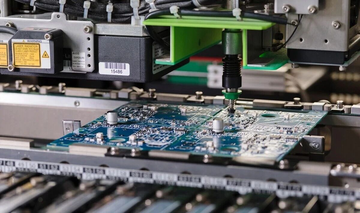
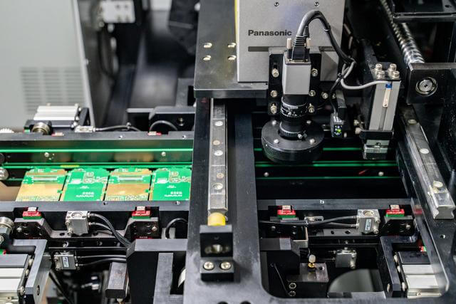
The DIP process is carried out after the SMT (surface mount technology) process, mainly for those large components that cannot be mounted by the machine. These components need to be inserted into the corresponding position of the PCB (printed circuit board) board by manual plug-in, and welded through wave soldering, and finally complete the assembly of the product. DIP plug-in process can be roughly divided into plug-in, wave soldering, cutting foot, inspection, testing and other processes.
Second,Steps in DIP
1. BOM Check and material preparation First, check and obtain the required materials according to the BOM (Bill of Materials) to ensure that the type and specifications of the materials are correct. Then, according to the process arrangement, components are allocated for each job and waiting for insertion.
2. DIP operations
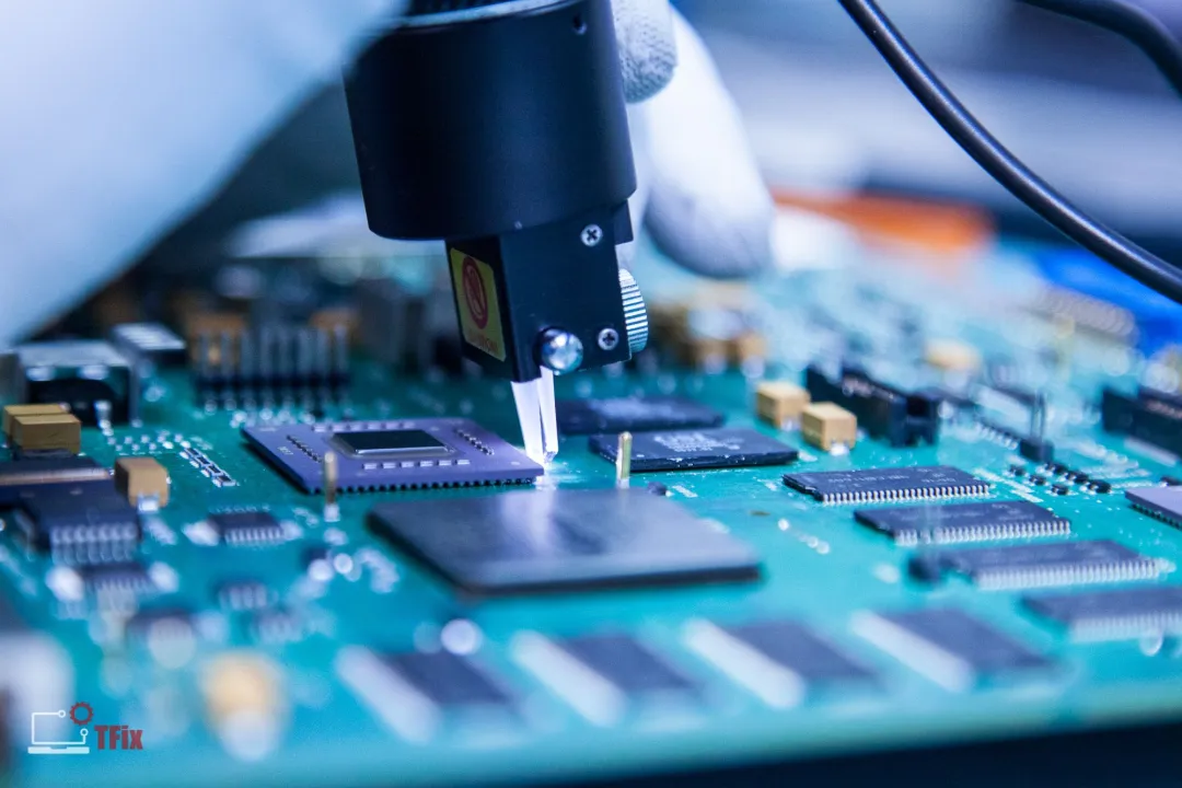
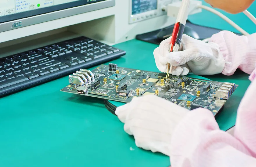
The plug-in is the first and crucial step in the DIP process. In this step, the component that needs to be perforated needs to be precisely inserted into the corresponding position of the PCBA board to prepare for over-wave soldering. During the plug-in process, you must pay attention to the following points:
1) Ensure that the surface of electronic components is free of oil stains, paint and other unclean substances, so as not to affect the welding quality.
2) Ensure that the electronic components and PCB board closely fit, no tilt, float or dislocation phenomenon, to ensure the accuracy and reliability of welding.
3) If there is a direction indicator on the electronic components, it is necessary to plug in the correct direction, do not plug in at will.
4) Pay attention to the strength of the plug-in to avoid excessive damage to components or PCB board.
Third, wave soldering process
1. Preparation before wave soldering Before wave soldering, you should carefully check whether there is excess flux or other impurities on the PCB board, and thoroughly remove it to prevent it from affecting the welding effect.
2. Wave soldering operation
Put the plug-in PCB board into the wave soldering conveyor belt, and complete the welding of the PCB board after spraying flux, preheating, wave soldering, cooling and other links. Wave soldering is a key step in DIP process, which is directly related to the solidity and quality of welding.
Four, cutting feet and post-treatment
1. Cutting foot treatment After the welding is completed, the PCBA board needs to be cut foot treatment to achieve the appropriate size. Be careful when cutting the foot to avoid damage to the welding joints.
2. Post welding and repair welding
For the PCBA board that is not completely welded or welded, manual repair welding is required to ensure that all components are solidly welded to the PCB board.
3. Wash the board
Finally, harmful substances such as flux remaining on PCBA finished products are cleaned to achieve the environmental cleanliness standards required by customers.
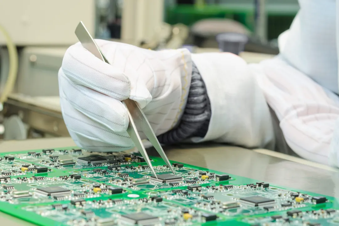
DIP plug-in process as an important link in PCBA manufacturing, each step of its operation is crucial. From the material preparation before the plug-in, the precision control in the plug-in process, to the fine operation of wave soldering, the meticulous treatment of cutting feet and post-processing, and then to the final inspection and testing, every link requires us to strictly check to ensure product quality. Only in this way can we lay a solid foundation for the performance and quality of electronic products to meet the needs of our customers.
