

In PCB (Printed Circuit Board) manufacturing, copper thickness refers to the thickness of the copper layer, which is typically measured in ounces (oz). 1 oz means the thickness achieved by evenly spreading 1 ounce of copper over an area of 1 square foot (ft²). The thickness of 1 oz copper is approximately 35um or 1.35mil.
Heavy copper PCB generally refers to PCBs with a copper thickness exceeding 3 ounces (105µm). In situations where routing space is limited and the current-carrying capacity of PCB traces cannot be improved by increasing trace width, using heavy copper PCBs can effectively meet the current-carrying requirements of the circuits while also improving the heat dissipation performance of thePCB.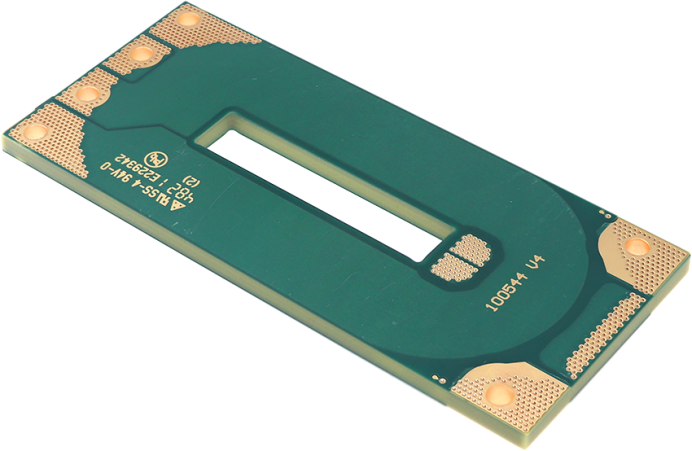
Core Advantages of Heavy Copper PCBs
1.High Current Carrying Capacity: Enables high current transmission within limited routing space, effectively increasing power density of equipment and supporting high-power circuit design requirements.
2.Efficient Thermal Conductivity and Dissipation: The thickened copper layer exhibits excellent thermal conductivity, rapidly dissipating heat generated during circuit operation while reducing PCB thermal deformation caused by temperature fluctuations, thereby greatly enhancing operational reliability.
3.Superior Mechanical Strength: The heavy copper layer reinforces the overall structural integrity of the PCB, improving resistance to deformation and wear, resulting in enhanced equipment durability.
Currently, heavy copper PCBs have been widely adopted in high-power, high-reliability applications such as communication base station power supplies, server power supplies, welding equipment, energy storage systems, automotive power systems, and aerospace.
II. How to estimate the required copper thickness for a PCB?
The following is the Conservative Chart provided by IPC-2152. The importance of the Conservative Chart is that it can address all situations, including internal and external conductors, PCB materials, PCB thickness, and environmental conditions such as air (except vacuum). The values obtained from this chart are very safe and valid under any circumstances (except vacuum environments), without considering other variables.
When engineers refer to the Conservative Chart for design, although it may not be optimal in terms of cost, area, etc., it can definitely meet the current and temperature rise requirements.
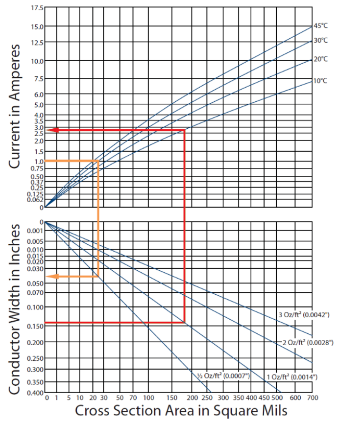
(IPC 2152 PCB power trace width vs. current and temperature rise relationship chart. Image source: Daniel Grillo)
The IPC-2152 Conservative Chart can be consulted to calculate PCB trace width and select the appropriate copper thickness.
As indicated by the red arrow, for a PCB trace width of 140 mil with 1 oz copper thickness, vertically locate the corresponding temperature rise requirement of 10°C, and then return to the y-axis to find the maximum allowable current of 2.75A.
As indicated by the orange arrow, if the PCB conductor needs to carry a current of 1A with a target temperature rise of 30°C, trace vertically downward to find the required trace width under different copper thicknesses. For example, when using 0.5 oz copper thickness, the trace width needs to reach 40 mil.
III. Core Manufacturing Processes for Heavy Copper PCBs
Compared to conventional PCBs, heavy copper PCBs present significantly greater processing challenges in etching, lamination, drilling, and solder mask application due to the increased copper layer thickness. Asinda Circuits has developed a dedicated production line tailored to heavy copper board characteristics, systematically addressing various processing difficulties to ensure product quality.
1. Etching Process
During heavy copper layer etching, low chemical solution exchange efficiency and substantial undercutting can easily lead to circuit pattern accuracy deviations. To address this, the industry employs multiple rapid etching cycles and optimized etching compensation coefficients to precisely control undercutting issues. Asinda Circuits is equipped with a dedicated heavy copper DES etching line capable of completing the etching process for up to 6 oz heavy copper PCBs in a single pass, delivering both precision and efficiency.
2. Lamination Process
Heavy copper PCBs feature deep circuit grooves. Under the same residual copper ratio, multiple types of high-flowability prepregs are required to ensure adequate resin filling of circuit gaps. Additionally, rivets are added to reinforce the core panels, mitigating the risk of panel slippage during lamination. Furthermore, the thick copper layer reduces the board's heating rate, necessitating extended holding time during the high-temperature stage to ensure complete curing of the prepreg.
Asinda Circuits employs Burkle fully automatic multi-layer lamination production lines with heavy copper-specific browning chemistry, combined with Mass LAM and Pin LAM hybrid processes, enabling stable mass production of heavy copper PCBs with up to 50 layers.
3. Drilling Process
For heavy copper PCBs with a board thickness exceeding 2.0mm, a step-drilling process is adopted with matched feed and retraction parameters. By reducing the entry speed, the process effectively prevents thick copper pad cracking and hole position deviations, ensuring drilling accuracy and quality.
4. Solder Mask Process
The significant height difference between heavy copper circuit traces and the substrate makes conventional solder mask processes prone to defects such as ink bleeding, insufficient ink thickness, exposed circuit copper (reddish appearance), pinholes, and air bubbles. The industry addresses these issues by diluting ink viscosity and employing multiple-layer screen printing processes.
Asinda Circuits is equipped with a fully automatic solder mask spray coating line, featuring a pretreatment + double-sided spray coating + pre-baking automated workflow, paired with dedicated high-pressure nozzles and high-viscosity specialty inks. This line can complete the solder mask spray coating for up to 4 oz heavy copper PCBs in a single pass, resulting in uniform solder mask layer thickness and excellent solderability.