

Via-in-pad technology enables compact BGA fan-out and optimizes PCB routing, effectively saving board space. However, it transfers solder joint reliability risks to PCB manufacturing, making plugging, planarization and copper capping processes the core determinants of soldering quality.
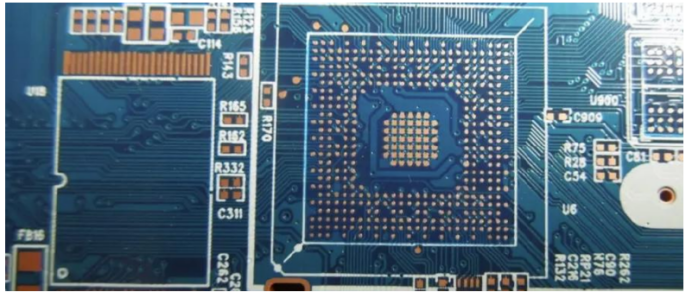
Ordinary vias placed inside BGA pads deliver shortest routing paths and neat layouts, yet pose hidden soldering risks. If vias are not fully filled and flattened, capillary action and surface tension will suck molten solder into hollow holes during reflow. This reduces effective solder volume on pads, causing subtle defects including insufficient solder, voids and intermittent cold solder joints. These flaws are concealed under BGA components, undetectable by visual inspection, and only exposed via X-ray scanning, cross-section analysis or temperature cycling tests.
Resin plugging is the mainstream solution, yet simple resin filling cannot guarantee qualified surfaces. Resin curing shrinkage creates dimples, while improper grinding causes raised protrusions. Uneven pad flatness disrupts stencil printing uniformity, leading to inconsistent solder paste distribution. Raised spots jack up solder balls, causing uneven compression on adjacent joints, while depressions result in insufficient solder, severely undermining BGA coplanarity and soldering stability.
Most design files only mark “via-in-pad” without specifying critical parameters, leaving manufacturers with uncertain process standards. Differences in hole aspect ratio, resin vacuum filling, copper capping thickness and flatness tolerance will lead to inconsistent finished pad quality across suppliers.
Do not rely solely on continuity testing for finished boards. Inspect pad flatness and hole opening appearance prior to BGA mounting. Use X‑ray scans after assembly to monitor solder‑ball volume, voids and offset. Add cross‑section analysis and reliability sampling to first‑article inspections for high‑current or thermally cycled circuits.
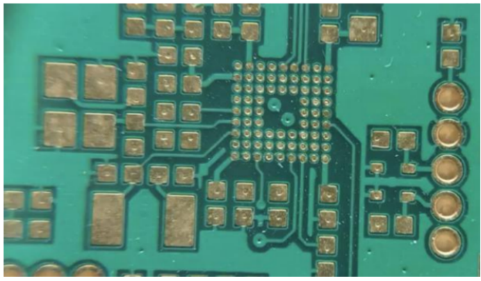
Investigate discoloration, dimples or fractured copper‑capping around hole openings on finished samples. Correlate design rules, manufacturer approvals, first‑article photos and soldering performance to isolate faults originating from layout, PCB fabrication or assembly reflow profiles.
For power and ground solder balls, evaluate current‑carrying capacity and thermal dissipation. Plugged vias and copper‑capping modify internal copper geometry. Thermal‑pad sizes, via arrays and solder‑ball thermal mass differ between power and signal terminals. Uneven heating rates between adjacent solder joints during reflow cannot always be resolved by enlarging stencil openings.
Flag via‑in‑pad BGA components as priority inspection items during mass production. Track X‑ray defect locations. Recurring faults aligned with specific rows or network traces indicate layout‑level thermal‑design flaws. Random defects require further investigation into fabrication batches, solder‑paste printing and reflow oven profiles.
Design phase: Explicitly specify via category, hole size, pad dimension and fabrication annotations.
Manufacturing phase: Secure signed‑off specifications for hole plugging, grinding, copper‑capping and flatness tolerances.
Validation phase: Perform pad‑surface inspection, X‑ray scanning and cross‑section verification for solder‑joint quality.
Conclusion
via-in-pad optimizes layout space but raises stricter requirements for PCB precision manufacturing. Standardized process definition and strict incoming inspection are essential to eliminate hidden cold solder joint risks.