

PCB warpage is a critical quality concern, typically driven by uneven stress distribution, differences in thermal expansion, mechanical stress during manufacturing, and inherent material properties.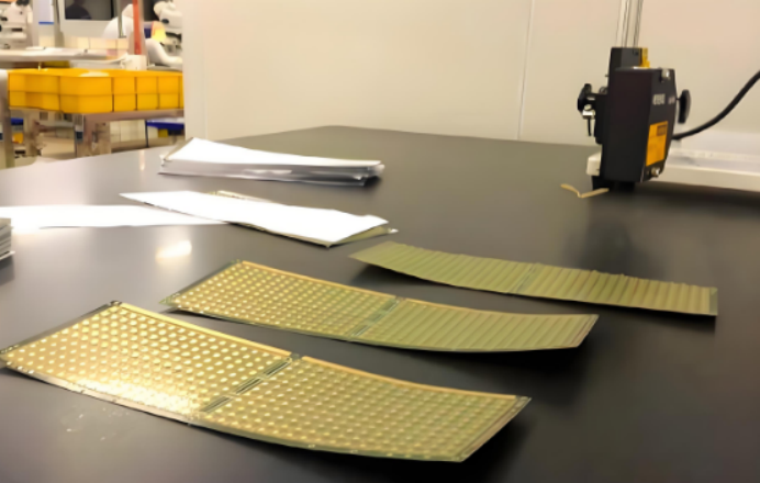
Measurement & Acceptance Criteria
The standard measurement method involves placing the PCB on a flat surface and using a feeler gauge to measure the gap at the four corners.
General acceptance criteria: Warpage ≤ 0.5% of the diagonal length.
For automotive electronics: Stricter tolerance of ≤ 0.3%.
Here are three key strategies to effectively manage and reduce PCB warpage:
1.Base Material & Auxiliary Material Optimization
• Material Selection: Prioritize low-CTE (Coefficient of Thermal Expansion) core laminates and prepregs that match the copper foil’s expansion rate to minimize thermal deformation. For thick or high-layer-count boards, use high-rigidity FR-4 and high-Tg materials for better thermal resistance and anti-deformation performance. For asymmetrical stack-ups, standardize the core/prepreg type, thickness, and resin content.
• Copper Balance: Ensure symmetrical copper area distribution between top and bottom layers. Avoid single-sided large copper pours or localized heavy copper. For heavy copper areas, utilize hatched or grid copper patterns to reduce localized stress concentration.
• Prepreg (PP) Control: Use the same batch and resin content for prepregs within a single panel to minimize curing shrinkage variations. High-resin PP is ideal for boards requiring high flatness, while low-resin PP helps reduce moisture-induced warpage.
2.PCB Layout & Design Optimization
• Symmetrical Stack-up: Maintain a perfectly symmetrical layer structure. Core thickness, prepreg ply count, copper weight, and trace distribution should be mirrored top-to-bottom. Avoid large bare areas or dense traces/pads on only one side.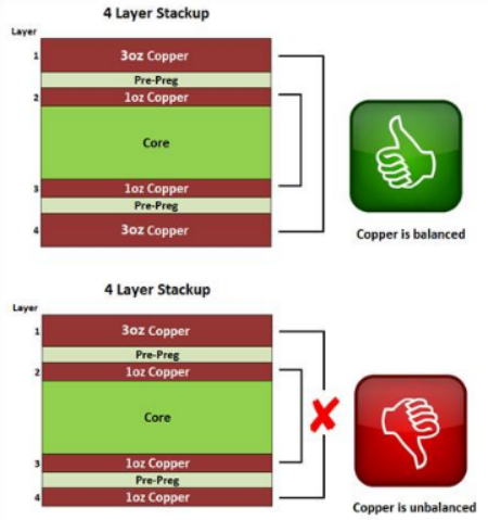
• Copper Pour & Pattern Layout: Split large solid copper pours into grid patterns (coverage ≥ 30%) to release thermal stress. Incorporate stress-relief slots or process openings along the board edges, especially for long or large panels. Avoid isolated large copper polygons around component or BGA areas.
• Panelization & Outline Design: Reduce single-side dimensions for large or elongated boards through rational panelization. Use connecting bars combined with stamp holes for panelization to minimize deformation during depanelization; avoid narrow, elongated connections. For thinner boards, increase the width of the process edges to enhance overall rigidity.
• Via Design: Distribute thermal relief and venting vias evenly across large areas to balance heat distribution and gas exhaust. Avoid clustering dense vias on one side of the board.
3.Manufacturing Process Improvements
• PCB Fabrication: Optimize lamination parameters, front-end processes (cutting, inner layer imaging, etching), surface finish processes, and baking procedures.
• SMT Assembly: Optimize reflow oven profiles, utilize carrier boards/fixtures, streamline material handling and transfer processes, optimize component placement sequencing, and implement post-reflow pressing/baking if necessary.
Successful PCB warpage control relies on combined optimization of materials, layout and manufacturing processes.