
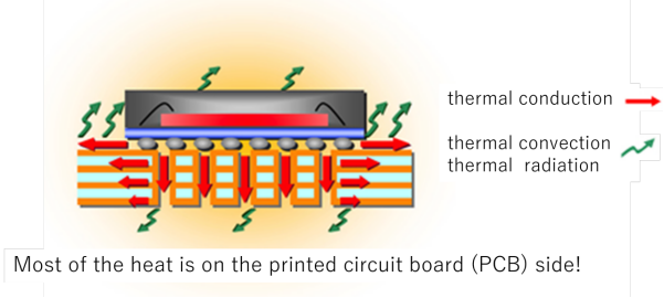
With the development of 5G, AIoT and high-performance computing, PCB design engineers are now facing unprecedented thermal challenges. The density of components is increasing, and devices are getting thinner. Traditional cooling methods (such as fans) are often limited by space.
The core problem: Heat accumulation can lead to fatigue of solder joints and PCB warping, ultimately affecting the reliability and lifespan of the product.
ASINDA's view: PCB should not merely be a carrier of electrical connections; it should also be part of an active thermal management system.
1. Core Thermal Strategies
Strategy 1: High-Conductivity Materials & Thick Copper: ASINDA utilizes high-purity electrolytic copper combined with precision etching processes. While maintaining fine pitch capabilities, we leverage inner power and ground planes as "thermal blankets" to achieve efficient in-plane heat diffusion.
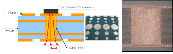
Strategy 2: Optimized Thermal Via Design: Through simulation, ASINDA optimizes the diameter, pitch, and filling process of thermal vias. This creates a "thermal highway" from the chip bottom to the PCB backside, effectively balancing thermal performance with electrical requirements (such as impedance control).
2. ASINDA’s Technological Highlights
3D Thermal Network via HDI: Utilizing advanced HDI (High Density Interconnect) technology, ASINDA employs micro-vias and buried vias to construct a three-dimensional thermal network. This effectively guides heat from the congested surface layer to the inner and bottom layers where there is more space for dissipation.
3. Simulation & Verification
Simulation-First Philosophy: ASINDA adheres to a "Simulation-First" approach. During the initial design phase, we utilize professional thermal simulation software (such as Ansys and Icepak) to model component power consumption and ambient temperatures, precisely locating hot spots. By iteratively refining stack-up designs and copper distribution, we ensure target temperatures are met before physical prototyping, saving clients significant rework costs.