
Mastering HDI PCB Manufacturing: Overcoming the Core Pain Points of Laser Drilling, Sequential Lamination, and Material Reliability
--Don't just trust the specs. See the internal quality. We analyze the cross-sections of Laser Drilling, Stacked Vias, and Lamination to show you exactly how to avoid failures.
As electronic devices shrink and performance requirements soar, High-Density Interconnect (HDI) PCBs have become the industry's go-to solution for miniaturization and signal integrity. However, the journey from design to manufacturable HDI boards is riddled with technical obstacles. For veteran engineers and manufacturing experts, understanding and mitigating these pain points is not just a best practice—it's a requirement for survival in a competitive market. This article dives deep into the three most critical pain points of HDI fabrication and presents actionable solutions to elevate manufacturing efficiency and product reliability.
Pain Point #1: Laser Drilling—The Devil is in the Detail
The Problem:
Microvia formation via laser drilling is the cornerstone of HDI technology, but it's fraught with risks. CO2 lasers (commonly used for blind/buried vias) require precise energy control to ablate the dielectric layer without damaging the underlying copper pad. Even a minor energy fluctuation can lead to:
Overablation: Burning through the copper pad, causing voids or delamination.
Incomplete Ablation: Dielectric residue at the via bottom, creating electrical resistance or open circuits.
Surface Roughness: Insufficient surface roughening post-ablation reduces copper plating adhesion, leading to poor reliability.
The Solution: Precision Engineering and Process Control
Laser System Selection: Hybrid UV/CO₂ lasers (e.g., Excimer or Nd:YAG lasers) offer finer control over pulse width and energy density, enabling sub-100μm via drilling with <±10μm accuracy.
Real-Time Energy Monitoring: Closed-loop systems with beam energy sensors and AI-based adjustments compensate for drifts, ensuring consistent ablation quality.
Surface Treatment Post-Drilling: Chemical etching (e.g., Plasma Desmear) or micro-roughening techniques (e.g., picosecond laser texturing) enhance the copper-plating surface for superior adhesion.
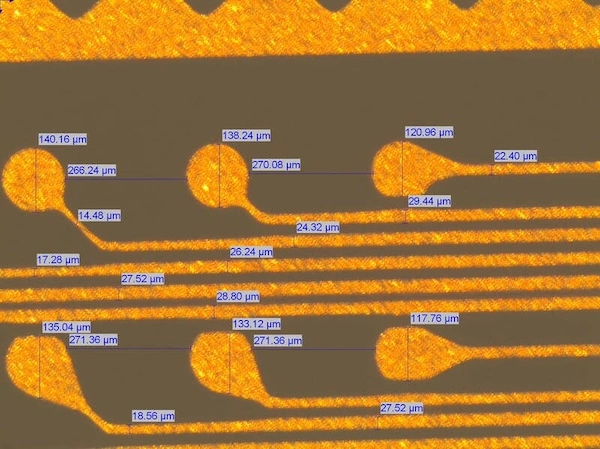
QC Checkpoints: Automated Optical Inspection (AOI) with >5μm resolution validates via diameter, aspect ratio, and absence of debris. IPC-6012 Class 3 standards demand via wall roughness <2μm and no voids >10μm.
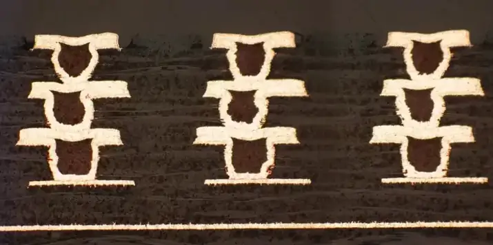
Pain Point #2: Stacked and Staggered Microvias—The Achilles' Heel of HDI
The Problem:
Stacked vias (e.g., 1+N+1 structures) offer routing flexibility but introduce significant reliability risks:
Thermal Cycling Failures: During SMT reflow (up to 260°C), differences in Coefficient of Thermal Expansion (CTE) between copper and substrate cause stress concentration at the via "neck," leading to cracks.
Via-Filling Challenges: Conventional electroplating struggles to fully fill deep, narrow stacked vias, creating voids that act as stress concentrators.
Electrochemical Migration: Moisture ingress into microcracks can cause Conductive Anodic Filament (CAF) growth, shorting adjacent traces.
The Solution: Material Science and Electrochemical Mastery
Via Filling Technology:
Conductive Epoxy Filling: Using silver- or copper-filled epoxies with vacuum-assisted injection to eliminate voids. Post-fill grinding ensures planarity.
Electroless Copper Plating: Optimized bath chemistry (e.g., low-stress additives) and pulse-reverse plating techniques deposit uniform copper layers down to 10μm via diameters.
Material Matching: Select substrates with CTE closer to copper (e.g., low-Dk Rogers materials vs. FR-4) to minimize thermal stress. Verify material Td (Thermal Decomposition Temperature) > 350°C for lead-free assembly.
Reliability Testing: Subject boards to Thermal Cycling (-55°C to 125°C, 1000 cycles) and Highly Accelerated Stress Test (HAST) to validate via integrity. IPC-TM-650 Method 2.6.26 measures CAF resistance.
Pain Point #3: Sequential Lamination—Precision in the Nano-Realm
The Problem:
HDI fabrication involves multiple cycles of layer build-up (e.g., 3+N+3), each introducing risks:
Registration Errors: Cumulative misalignment across lamination cycles can exceed IPC Class 2/3 tolerances, causing via-to-pad misregistration >25μm, severing connections.
Dielectric Thickness Control: Varying resin flow during press cycles results in non-uniform layer thickness, impacting impedance control in high-speed designs.
Void Entrapment: Air pockets trapped between layers during bonding create delamination hotspots, especially in fine-pitch BGA areas.
The Solution: Machine Vision, Materials, and Process Discipline
Advanced Registration Systems:
Laser Etched Fiducials: Replace traditional mechanical punches with laser-etched fiducials (±5μm accuracy) to account for material shrinkage.
Automated Optical Alignment: Machine vision systems with <1μm repeatability align inner layers during lay-up.
Press Parameters Optimization:
Pressure-Temperature Profiles: Use multi-stage curing cycles (e.g., ramp-up to 200°C at 1.5°C/min) with vacuum lamination to expel trapped air.
Prepreg Selection: Low-flow/high-resin-content prepregs (e.g., ABF films) minimize resin squeeze-out while maintaining insulation.
Impedance Assurance: Post-lamination, verify trace impedance with Time-Domain Reflectometry (TDR) testing and adjust dielectric thicknesses as needed to meet ±10% spec.
The Role of Data-Driven Manufacturing (DDM) in HDI
For true mastery, manufacturers must embrace Industry 4.0 tools:
Real-Time Process Monitoring: Connect laser drills, laminators, and plating lines to IIoT systems to capture parameters (e.g., energy density, pressure profiles) in real-time.
Predictive Analytics: Machine learning models analyze process data to predict defects (e.g., via voids) before they occur, enabling proactive adjustments.
Digital Twins: Simulate lamination cycles and material behavior using finite element analysis (FEA) to optimize designs for manufacturability.
Conclusion: Pain Points as Gateways to Excellence
The transition to HDI manufacturing is not for the faint-hearted. However, by embracing these pain points as opportunities for innovation, manufacturers can:
Minimize Scrap Rates: Tighter process control reduces rework costs by up to 30%.
Differentiate with Quality: Boards passing stringent thermal cycling and CAF tests command premium pricing.
Future-Proof Operations: Mastery of HDI today prepares fabs for next-gen technologies like Any Layer HDI (ALIVH) and embedded components.
In HDI, the industry’s "gold standard" is defined not by theoretical knowledge, but by the ability to solve these exacting pain points at scale. Leveraging micro-hole engineering solutions, Asinda has established a reputation for excellence in the aerospace, automotive, and medical sectors, earning the trust of even the most demanding clients.