
Driven by 5G, AI servers, and 400G/800G optical modules, high-speed PCB design has entered an era of "micron-level" competition. As data rates surpass 56Gbps, engineers are looking beyond just Dielectric Constant (Dk) and Dissipation Factor (Df). A more subtle parameter is emerging as the make-or-break factor: Copper Foil Surface Roughness (Rz).
Why "Smoothness" Matters
At high frequencies, current is confined to a thin layer on the conductor's surface due to the Skin Effect. At 25GHz, the skin depth of copper is merely 0.42μm. If the foil's roughness (Rz) exceeds this depth, the current is forced to travel a longer, winding path along the microscopic peaks and valleys. This increases effective resistance, causes impedance discontinuities, and leads to severe signal attenuation and phase distortion.
The Evolution of Copper Foil Technology
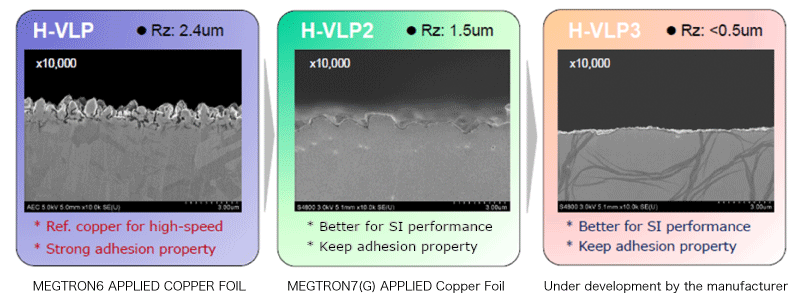
H-VLP (Rz≈2.4μm): The "entry-level" for high-speed materials, balancing adhesion with performance. Suitable for applications below 10Gbps.
H-VLP2 (Rz≈1.5μm): By optimizing oxide treatment, this grade significantly reduces conductor loss while maintaining peel strength. It is the current mainstream choice for 25G/56Gbps backplanes.
H-VLP3 (Rz<0.5μm): Representing the future of "ultra-smooth" tech, its near-mirror surface minimizes skin effect losses. However, the challenge lies in reliability; extremely low roughness can weaken the bond with prepreg, increasing delamination risks. It is currently in a trade-off stage between ultimate performance and mechanical robustness.
Asinda's Strategy
Precise Selection: For 112Gbps PAM4 signals, H-VLP2 or H-VLP3 is recommended, paired with low-Df (M6/M7 grade) laminates.
Process Synergy: Collaborate closely with PCB fabricators to ensure lamination parameters (temp/pressure) are tuned for low-profile foils to prevent adhesion failures.
Every micron of progress in copper foil technology paves the way for the next generation of data speeds.
#PCBDesign #SignalIntegrity #HighSpeedDigital #5G #MaterialsScience #HardwareEngineering