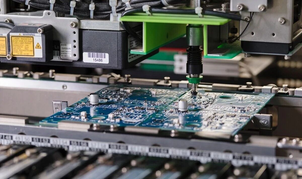

Cryogenic applications involve the utilization of extremely low temperatures, typically below -150°C or -238°F, for various scientific, industrial, and technological purposes. These environments pose unique challenges and necessitate specialized approaches, particularly in the design of printed circuit boards (PCBs). As the backbone of electronic systems, PCBs play a pivotal role in ensuring the functionality and reliability of components and devices in cryogenic conditions.
Importance of PCB Design in Cryogenic Environments
Traditional electronic components may not perform reliably or may even fail outright under the harsh conditions of extreme cold. PCBs must be tailored to withstand low temperatures, ensuring the integrity of electrical signals, thermal stability, and overall system functionality. The challenges presented by cryogenic applications underscore the need for a comprehensive and specialized approach to PCB design, encompassing material selection, thermal management, signal integrity, and reliability considerations.
Challenges in Cryogenic PCB Design
Material Challenges
1.Substrate Material Selection: Designing PCBs for cryogenic environments requires careful consideration of the substrate material. Traditional materials may become brittle or experience significant changes in electrical properties at extremely low temperatures. Polyimide and PTFE-based substrates are commonly favoured for their low thermal expansion coefficients and reliable performance in cryogenic conditions.
2.Copper Conductor Considerations: Copper, a standard material for PCB conductors, can face challenges in cryogenic applications. At cryogenic temperatures, copper still has residual resistance, affecting the electrical performance of the PCB. High-purity copper or copper alloys designed for cryogenic use are preferred to mitigate these effects. Additionally, the differential thermal expansion between copper conductors and the substrate should be carefully managed to prevent mechanical stress on the PCB.
Component Challenges
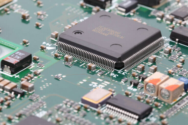
1.Cryogenic-Grade Component Selection: Standard electronic components may not operate reliably or efficiently in cryogenic conditions. Cryogenic-grade components are engineered to maintain their functionality and electrical characteristics at extremely low temperatures. These may include transistors, resistors, capacitors, and other active and passive components with suitable cryogenic specifications.
2.Dielectric Compatibility: The dielectric materials used in components, such as capacitors, must be compatible with cryogenic temperatures. Some dielectrics may undergo phase changes or exhibit altered electrical properties in extremely low temperatures, impacting the performance of the overall PCB.