
The PCB layout is complete, the components have been selected, and the Gerber files have been sent to the PCB manufacturer. But when it comes to the production stage, have you ever wondered why some components are soldered using reflow ovens while others require wave soldering? After all, both processes involve melting solder to attach components to the PCB—so why does the production line need two different types of equipment?
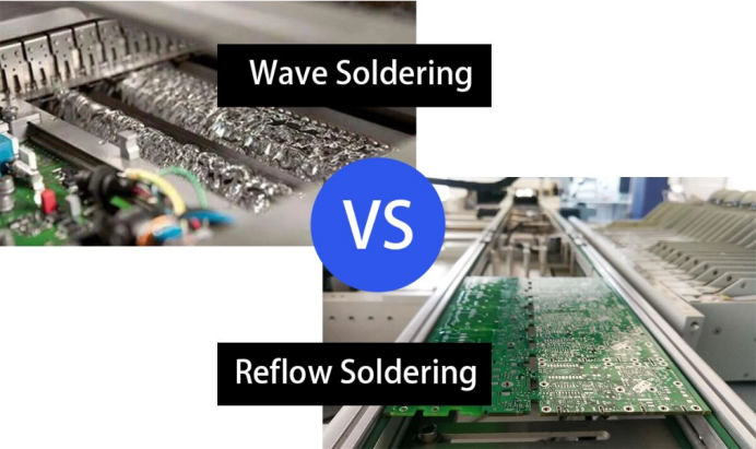
The biggest difference between reflow soldering and wave soldering lies in how the solder material reaches the joint, as well as the types of components each process is best suited for. For hardware engineers, understanding these two processes is not just a matter of expanding knowledge; PCB layout, package selection, pad design, and even subsequent failure analysis can all be influenced by them.
Reflow soldering involves first printing solder paste and then heating the entire assembly.
Reflow soldering is primarily used for SMT surface-mount components, such as resistors, capacitors, SOPs, QFNs, BGAs, and others.
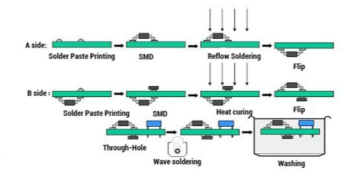
Its basic process is as follows: first, solder paste is printed onto the PCB pads; then, components are mounted; finally, the entire PCB passes through a reflow oven. During this process, the solder paste undergoes preheating, temperature ramp-up, dwell above the liquidus temperature, and cooling, completing melting, wetting, and solidification. An often-overlooked detail is that reflow soldering does not simply heat the entire PCB to a fixed temperature and stop—instead, it requires precise control of how the temperature varies over time.
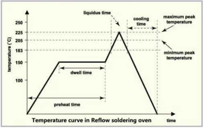
Taking the commonly used SAC305 lead-free solder as an example, its melting point is approximately 217°C, and the actual reflow profile typically causes the solder to…
The temperature should be raised above the liquidus line and held there for a specified duration; however, the exact peak temperature, the time spent above the liquidus line, and the heating/cooling rates must be determined based on the solder paste, the temperature rating of the components, and the thermal capacity of the PCB
Wave soldering involves bringing molten solder into direct contact with the PCB solder joints.
The operation of wave soldering is much more straightforward: the equipment melts the solder and uses a pump to generate a steady solder wave. After the PCB has been treated with flux and preheated, its soldering surfaces come into contact with the molten solder, completing the joint between the leads and the pads.
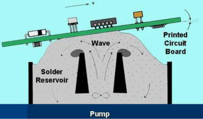
Its most classic application is through-hole components, such as through-hole connectors, transformers, relay sockets, and certain high-power devices. The component leads pass through the PCB’s vias, and solder on the soldering side of the board flows over the leads and pads, forming solder joints via wetting.
Why can’t all PCBs simply be passed through wave soldering?
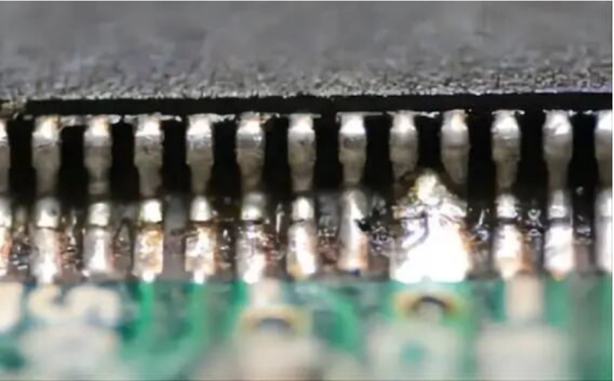
Because wave soldering involves direct contact between the solder and localized areas of the PCB, if the board contains a large number of surface-mount components—especially those with fine-pitch leads or bottom side pad packages—the solder may form bridges between adjacent pins, and it may also cause components that are not suitable for wave soldering to overheat or experience poor solder joints.
In addition, wave soldering must take into account the PCB’s direction of travel, pad spacing, solder mask design, lead out length, and component placement on the soldering side. If the design is suboptimal, even perfectly tuned equipment parameters will struggle to ensure stable mass production. It is important to emphasize that reflow soldering is not limited to surface mount components, nor is wave soldering restricted to through hole parts. In actual production, processes such as selective wave soldering and through hole reflow soldering are also employed; the choice of method should be determined by factors including package geometry, component density on the board, solder joint reliability, and production capacity requirements.
For hardware engineers, these design details are what really matter.
First, when evaluating packages and pads, one cannot focus solely on electrical connectivity. Packages such as QFN and BGA impose specific requirements on solder paste printing, pad design, and reflow profiles, while through-hole pads must account for hole diameter, copper thickness, lead dimensions, and solder fill.
Second, large copper pours can alter the thermal distribution during soldering. If the pads of power components are connected to extensive copper areas, heat may be rapidly dissipated, potentially leading to insufficient local heating. During design, it is essential to verify this by considering thermal mass, pad geometry, and actual temperature profiles, rather than simply increasing the reflow oven temperature.
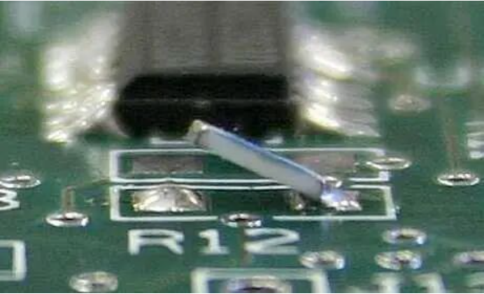
Third, production defects are not necessarily due to component quality issues. For example, resistor tombstoning after reflow soldering may result from uneven heating of the two pad surfaces, variations in solder paste volume, or placement misalignment. Similarly, connector pin bridging after wave soldering may be attributable to pad spacing, pin orientation, flux characteristics, or wave soldering process parameters.