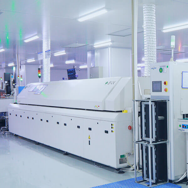
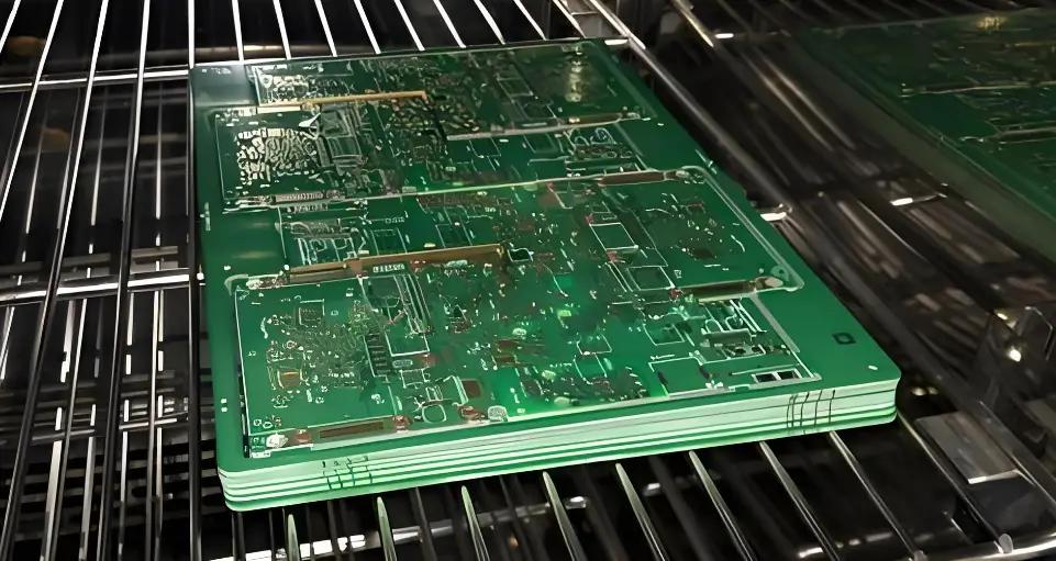
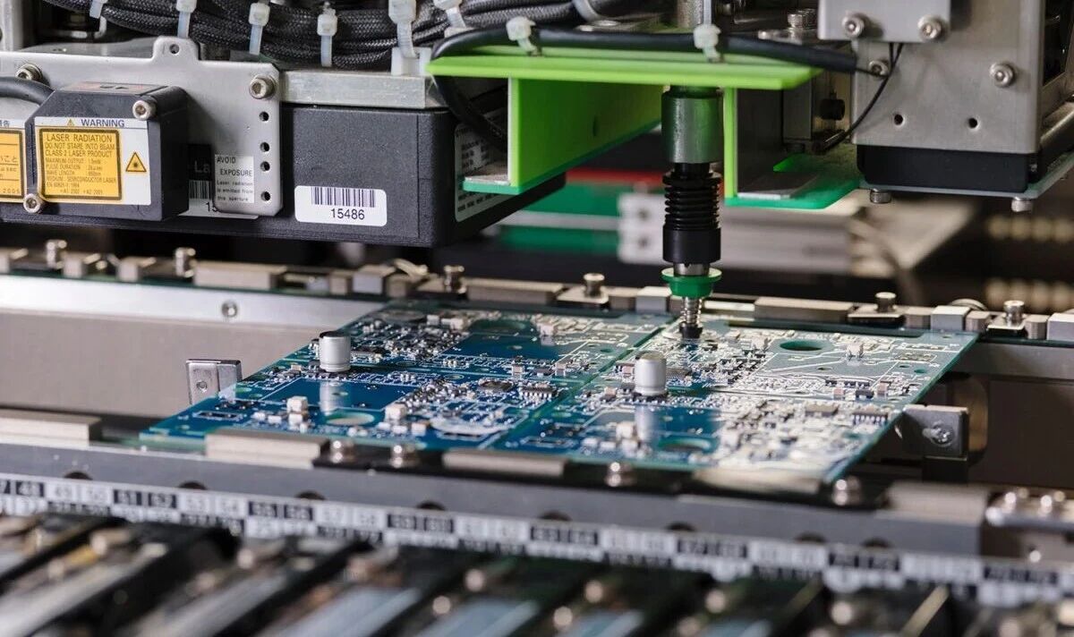
Pinholes or gas holes in wave soldering are primarily caused by gas release during the welding process, often related to copper plating thickness. When moisture inside the PCB is heated and turns into gas during welding, it escapes through the molten solder. As the solder solidifies, continued gas release forms voids, leading to temporary conductivity that may degrade over time.
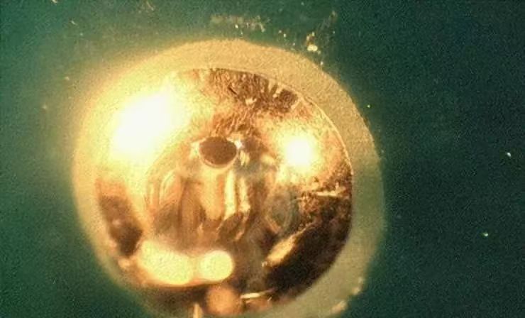
Gas holes
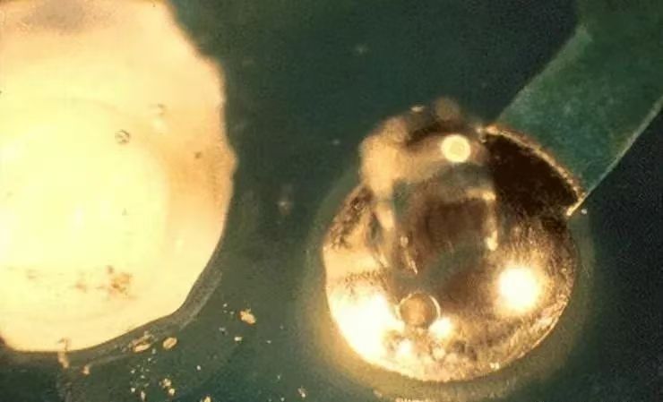
Pinholes
Gas holesPinholes
1.Causes
1.The top temperature of the PCB is too low.
2.Excessive moisture accumulated in the circuit board tries to escape through the thin copper plating.
3.Similar types of components are not oriented in the same direction, resulting in poor copper plating quality.
4.The ratio of lead to hole is either too small or too large.
2.Solutions
1.Increase the quality of the circuit board by plating at least 25 microns of copper in the via holes.
2.Baking is usually used to dry the board and eliminate the gas problem, but it does not solve the root cause.
3.Preventive Measures
Verify the top PCB temperature, verify the deposition of solder flux and the required preheating temperature, and check the moisture in the laminate. Perform pre-baking if necessary, but check the via plating.
When we do preventive work well, pinholes and gas holes can be avoided, ensuring high-quality industry development.


