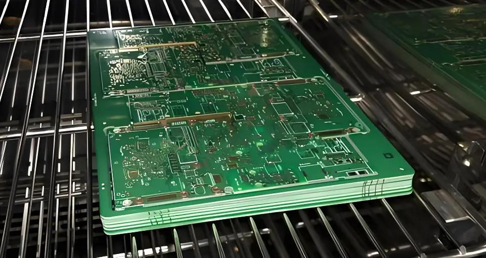

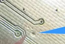
In the PCB manufacturing process, poor pressing is one of the main causes of dent problems. Poor pressing is usually caused by uneven pressure, material quality issues, equipment failures, or improper operations. The following is a detailed analysis and solutions for dent problems caused by poor pressing in PCB manufacturing: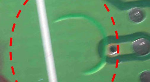
 I. Cause Analysis
1.Uneven Pressure:During the pressing process, uneven pressure distribution can cause local overloading on the circuit board, resulting in dents. This may be due to the low precision of the pressing equipment or improper operation
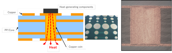
2.Material Issues:Poor-quality pressing materials (e.g., copper foil, resin) can lead to insufficient interlayer adhesion, affecting the pressing effect. For example, a mismatch between copper foil and resin systems can reduce peel strength, causing dents during pressing
3.Improper Operations:Misalignment of the upper and lower boards during lamination or excessive operating pressure can also lead to dent formation
II. Solutions
1.Optimize Pressing Processes:
Use high-quality pressing materials with strict screening and control
Apply uniform pressure using rollers or flat presses to ensure even distribution
Optimize lamination processes to ensure sufficient and uniform resin flow, avoiding air entrapment
2.Improve Material Selection:
Use high-cohesion and low-porosity substrates to enhance interlayer adhesion
Select resin systems compatible with copper foil to improve peel strength
3.Quality Control and Inspection:
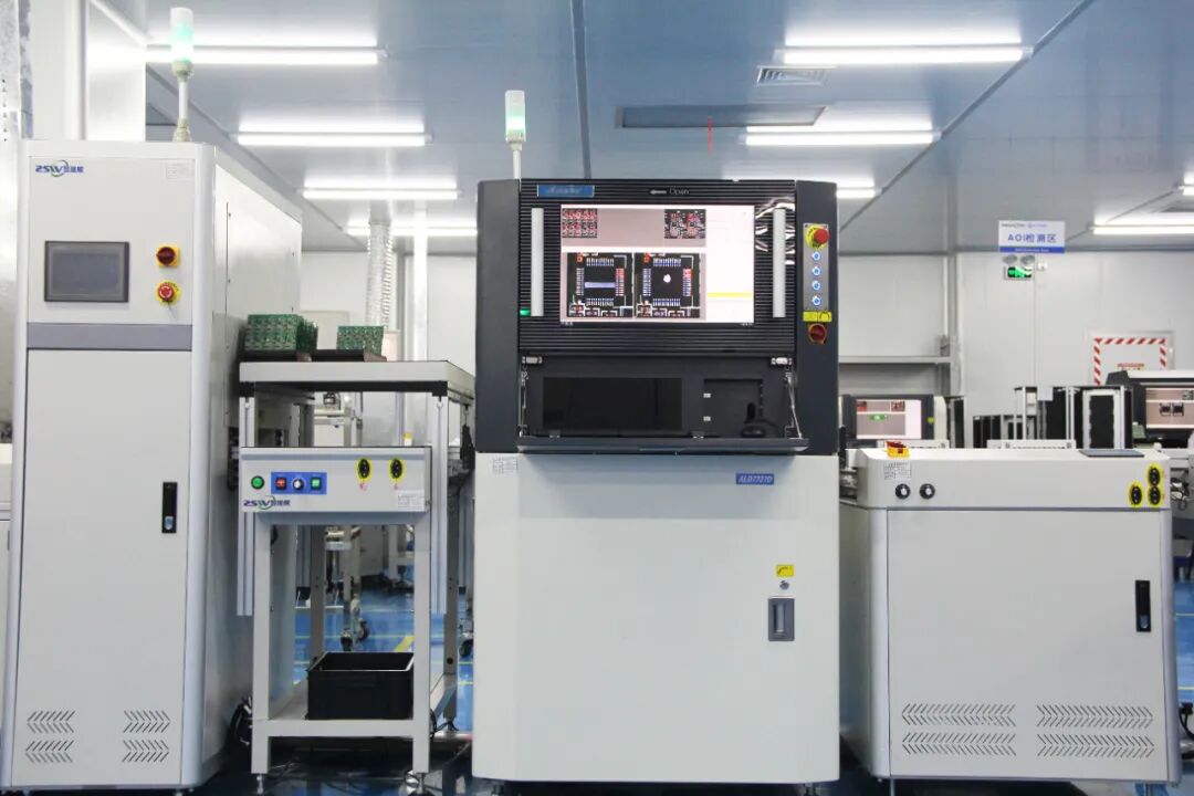
Employ automatic optical inspection (AOI) and other technologies for real-time defect detection and handling
Implement strict quality checks throughout the entire production process, from raw materials to finished products
These measures can effectively reduce dent problems caused by poor pressing in PCB manufacturing, enhancing product quality and reliability.